Welcome to Ken-Hub!
An all-encompassing resource for contemporary technical advancements and trending subjects.


Science

Technology

Engineering

Management
Energy Dispersive X-Ray Spectroscopy (EDS)
What is EDS ?
Energy Dispersive X-ray Spectroscopy (EDS), also known as EDX or XEDS, is an advanced technique for microanalytical investigation of the chemical composition of a material. It provides both qualitative and quantitative information about elements with atomic numbers (Z) greater than 3, and in some specific configurations, it can detect elements with Z greater than 2.
The EDS process involves directing an electron beam onto the sample, either within a scanning electron microscope (SEM) or a transmission electron microscope (TEM). As the primary electrons from the beam interact with the atoms in the sample, two types of X-rays are generated: Bremsstrahlung X-rays, often referred to as background or continuum X-rays, and Characteristic X-rays. An Energy Dispersive detector captures these X-rays, generating a spectrum (histogram) that displays the intensity (X-ray count rate) against energy. In the past, EDS detectors were primarily based on Si(Li) detectors cooled with liquid nitrogen, but contemporary systems now incorporate silicon drift detectors (SDD) with Peltier cooling systems. By analyzing the X-ray energies, the elements present in the sample can be identified, while the intensity of the X-ray peaks allows for quantification of element concentrations.
The underlying principles of X-ray generation and detection in EDS remain consistent for both SEM and TEM, but there are performance differences due to variations in microscope construction and the use of different accelerating voltages. The spatial resolution of EDS analysis highly dependent to the interaction volume size, which in turns controlled by the accelerating voltage and the atomic number (Z) of the sample. For instance, the element to be analysed generate characteristic x-rays at certain accelerating voltage, if we provide lesser accelerating voltage to the sample, the element may not be dtetcted. Typically, spatial and depth resolutions on the order of a few microns are achieved. In contrast, in TEM, the spatial resolution is significantly better at higher accelerating voltages due to the thin foil sample and reduced electron beam spreading, resulting in resolutions on the order of nanometers, with depth resolution governed by the sample thickness. The detection limit of EDS analysis in SEM depends upon the composition of sample, which falls within the range of 0.1-0.5 wt%, in general. While EDS is effective for major and minor element analysis, it may lack the sensitivity required for trace-element analysis. On the other hand, EDS analysis in TEM can achieve detection limits of approximately 0.01-0.1 wt%.
It's worth noting that EDS is considered a non-destructive analytical technique, allowing the sample to be re-analyzed multiple times. However, some materials, such as clay minerals and glasses, can experience damage under the electron beam, making them more susceptible to alteration. For qualitative analysis, specific sample preparation beyond that required for SEM or TEM imaging is generally unnecessary. However, for quantitative analysis in SEM, the sample must be bulk, flat, and polished.

How it works ?
Electron microscopes analyze specimens composed of atoms. When the primary beam of electrons focuses on a specimen, it penetrates the material and interacts with the constituent atoms. In a scanning electron microscope (SEM), the primary beam electrons spread out within the sample, forming an interaction volume. The size of this interaction volume is influenced by the accelerating voltage of the primary beam and the mean atomic number or density of the sample. A higher accelerating voltage leads to a larger interaction volume, whereas samples with a higher mean atomic number result in a smaller interaction volume.

Generation of characteristic X-ray
In both the SEM and TEM, the interaction of the electron beam with the sample generates two types of X-rays: Bremsstrahlung and Characteristic X-rays. Bremsstrahlung X-rays, also known as continuum or background X-rays, result from the primary beam electrons slowing down due to the electric field surrounding the atoms in the sample. These X-rays have a range of energies, from 0 up to the energy of the primary electrons. The intensity of Bremsstrahlung X-rays at any energy E is governed by Kramers' Law, where it is proportional to the electron probe current and the mean atomic number (Z) of the specimen.

On the other hand, Characteristic X-rays are produced by electron transitions between the inner electron shells of the atoms in the sample. When an electron from the primary beam removes an electron from an inner shell, creating an ionized and unstable state, an outer shell electron fills the vacancy, emitting an X-ray photon. The energy of the emitted X-ray is equal to the difference between the ionization energies of the involved electrons. The production of Characteristic X-rays can occur from irradiation by primary beams of protons (PIXE), X-rays (XRF), or electrons (EDS). The atoms in the sample consist of a nucleus made up of neutrons and protons, surrounded by a cloud of electrons. Each element is defined by the number of protons in its nucleus, which gives its atomic number (Z). In a neutral atom, the number of protons is balanced by the number of electrons. The electrons occupy energy levels known as electron shells, with the K shell being the closest to the nucleus, followed by L, M, N, O, P, and Q shells. EDS microanalysis mainly focuses on the K, L, and M shells, which contain a maximum of two, eight, and eighteen electrons, respectively. Each shell is further divided into subshells, each with slightly different electron energies. The ionization energies for each shell and subshell are specific to each element. Characteristic X-ray lines are named using the Siegbahn notation, indicating the involved element (e.g., Cu), the ionized electron shell (e.g., K, L, or M), and the relative intensity of the line within each shell (e.g., α, β, or γ). The lines within each shell form a family or series of X-ray lines, such as the K family with Kα and Kβ X-ray lines.
The energy of Characteristic X-ray lines for each element has a connection with its atomic number. This energy is directly proportional to the square of the atomic number, Z. As the atomic number increases, the energy of X-ray lines like Kα also increases in the energy-dispersive (ED) spectrum. This relationship is known as Moseley’s Law, discovered by Henry Moseley in 1913. An alternate system for labeling Characteristic X-ray lines is suggested by IUPAC. In this system, each line is identified by the from-shell or subshell and the to-shell or subshell transition, for example, Cu K1-L1, where an X-ray is emitted due to the movement of an electron from the L1 shell to the K1 shell. Despite the clarity of the IUPAC naming system, the scientific community and industrial applications still tend to use the conventional method to designate X-ray characteristic peaks in EDS.
Factors affecting X-ray characteristics
The amplitude of the Characteristic X-ray peaks in an ED spectrum, or the X-ray intensity, can be expressed in terms of X-ray counts or count rate (counts per second or cps). While it might be assumed that the height of an X-ray peak corresponds to the concentration of the element in the sample, this assumption is not universally accurate. While TEM-generated spectra often follow this trend, SEM-generated spectra can be influenced by various factors related to the sample, X-ray generation process, and detector characteristics. Consequently, the intensities of X-ray peaks are not directly proportional to element concentration. However, it remains true that the concentration of an element in the sample does impact the peak height. Major elements (> 10 wt. %) exhibit prominent peaks, whereas minor (1-10 wt. %) or trace elements (<1 wt. %) display smaller or even undetectable peaks.
The beam current or probe current reflects the quantity of electrons in the primary electron beam of an electron microscope, regulated by the condenser lens or spot size control. The number of X-rays generated and recorded in the X-ray spectrum is directly linked to the number of electrons in the primary beam. Although raising the beam current increases X-ray generation, it does not alter the relative intensities of Characteristic X-ray peaks in the spectrum.
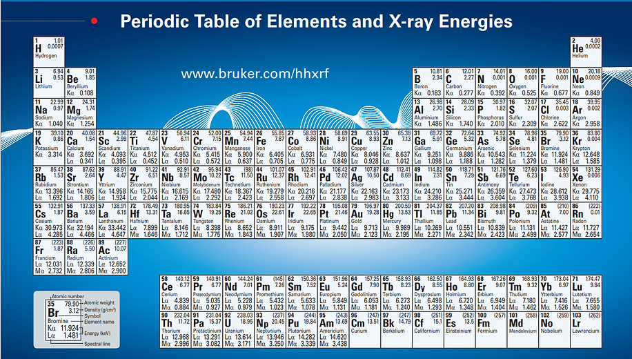
The energy of electrons in the primary beam is governed by the accelerating voltage in the electron microscope. SEMs generally use accelerating voltages of 5-30 keV, whereas TEMs employ much higher voltages of 100-400 keV or more. To induce Characteristic X-rays, the energy of the primary beam electrons must exceed the ionization energy (critical ionization energy) of the inner-shell electrons within the sample's atoms. While TEMs easily meet this requirement due to their high accelerating voltages, SEMs must carefully select a sufficiently high accelerating voltage to stimulate X-ray emissions from all sample elements. The critical ionization energy of various elements is presented in the periodic table below (sourced from Bruker’s periodic table for elements and X-ray energies). As an example, consider a sample containing Fe, Cu, and Al elements, with respective critical ionization energies for Kα being 6.405 keV, 8.046 keV, and 1.486 keV. When an accelerating voltage of 1 keV is applied to the sample, no Kα X-ray line will be emitted. At 7 keV, only Al and Fe will generate Kα X-rays, and at 9 keV, Kα X-rays will be produced for all elements. Nevertheless, it's important to note that an optimal overvoltage is required to ensure the precise generation of X-rays for accurate element identification. This ratio compares the energy of the electrons in the primary beam, denoted as Eo, with the critical ionization energy, Ec. The latter is the energy needed to ionize an inner shell of an atom within the sample. For instance, when the accelerating voltage is set at 15 keV, the energy of electrons in the primary beam amounts to 15 keV. Considering the critical excitation energy of Cu Kα X-rays as 8.046 keV, the resulting overvoltage ratio (U = Eo/Ec) is calculated as 1.86. Efficient X-ray generation requires an overvoltage ratio of at least 2, although the optimal value often stands at 2.7. This optimal ratio ensures the ideal conditions for generating X-rays, facilitating accurate elemental analysis.

How it measures ?
The primary method employed in both SEMs and TEMs to identify the generated and emitted X-rays from a sample is the energy-dispersive X-ray analysis system (EDS, EDX, or XEDS). While for specialized applications, alternative detection systems like wavelength dispersive spectrometers (WDS) or microcalorimeters might find use. Despite variations across EDS analysis systems due to factors such as age and manufacturer, they generally consist of three fundamental components: a detector, a pulse processor, and a multi-channel analyzer or display.
The detection mechanism relies on a semiconductor device, usually a silicon crystal, although intrinsic germanium detectors have been utilized in TEMs. Initially, the commercial systems in the late 1960s featured lithium-drifted silicon (Si(Li)) detectors; however, silicon drift detectors (SDD) have now supplanted them. When X-rays interact with the detector crystal, they generate a charge converted into a voltage pulse, which is then sent to a pulse processor. This processor eliminates signal noise, differentiates incoming X-ray energies, and distinguishes nearly simultaneous X-ray arrivals. Noise reduction is achieved by signal averaging in the pulse processor. The averaging time is adjustable through the system's time constant or processing time. Longer processing times enhance spectral resolution, crucial for quantitative analysis. Shorter times suit tasks prioritizing X-ray numbers, such as mapping. However, extended processing increases dead time, during which the system doesn't count incoming X-rays but processes existing signals. Dead time is also influenced by X-ray count rate. High counts overwhelm the processor, rejecting X-rays. Si(Li) detectors work at 5,000 to 20,000 cps with dead times of 20-30%. SDDs are preferred due to their ability to handle count rates above 100,000 cps and dead times up to ~50%. Count rates are optimized by adjusting beam current and process time for an acceptable count rate and detector dead time, with desired spectral resolution.
The pulse processor's output is channeled to a multi-channel analyzer or computer display. The energy range of the spectrum is segmented into channels, e.g., 1024, 2048, or 4096, each with energy widths like 5, 10, or 20 eV. The count of X-rays with specific energy attributes is allocated to respective channels, forming a histogram showcasing intensity (X-ray count) against energy.
Qualitative Analysis
Qualitative analysis entails identifying the elemental composition and distribution within an unknown sample, without providing details about the abundance of each element present. It's important to note that commercially available measurement systems are not very accurate; they might detect elements that aren't actually present or overlook elements that are there. Thus, it becomes very crucial to verify the obtained result from EDS qualitative analysis.

The energies of Characteristic X-rays emitted by elements in a sample provide a means of identification. Nevertheless, the presence of overlapping peaks from different elements introduces complexity, making accurate identification reliant on distinguishing peaks within distinct X-ray families. The consistent relative weights and energies of the characteristic X-ray lines enable the recognition of related peaks in the X-ray spectrum. Beyond 4 keV, the K and L families are distinguishable. The K family includes Kα and Kβ peaks, with intensity ratios of approximately 10:1. However, Kα can be further divided into Kα1 and Kα2, often overlapping and thus recognized as Kα peaks only. The L family involves six visible lines, with the Ll line forming a minor peak from electron transitions between M I and L III subshells. The Lα, Lβ1, and Lβ2 lines constitute a series of three peaks with decreasing magnitudes and relative intensities of about 10:7:2. The Lγ1 and Lγ3 lines create minor peaks on the high-energy side. M family peaks are absent above 4 keV. Generating and Identifying correct peaks involves these factors:
-
SEM: For stable sample under high vacuum and not damage-prone, use 15-30 kV.
-
TEM: To collect sufficient X-ray counts for analysis, generally at highest accelerating voltage.
-
Lower accelerating voltage if sample susceptible to damage. Lower energy X-rays for identification of certain elements (e.g., L or M lines for Z > 20).
-
Adjust beam current to minimize sample damage yet generate enough X-rays for reliable identification.
-
Optimize electron beam-sample-detector geometry and working distance.
-
X-ray detector close to sample for maximizing X-ray collection.
-
Conductive samples need no coating; insulating samples may require coating for conductivity.
-
Conductive coating materials (Carbon, Au, Pt) may introduce X-rays in ED spectrum. Carbon is preferred as it minimizes spectral interferences.
-
Ensure at least two distinct peaks for both K and L families for identification and related minor peaks.
-
If L family peaks exist, low-energy M family peaks should be present.
-
If K family peaks are present, lower-energy L family peaks should be present.
-
Unidentified peaks below 4 keV are likely K family peaks.
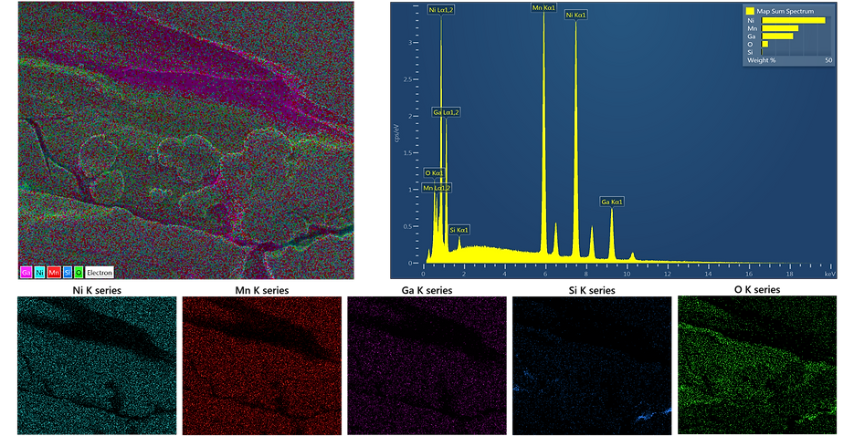
Below is the example of quantitative analysis of Ni-Mn-Ga samples.

Quantitative Analysis
In quantitative analysis the weight fraction of each detected elements are determined by comparing the X-rays with the data measured from standard reference materials, i.e. EPMA analysis, and hence called standardized quantitative analysis process. In non-standard or semi quantitative analysis, the X-ray spectra are compared with data collected from standards in the factory of the manufacturer of the EDS system and stored with the system software. However, with the area mapped images, the image processing software such as ImageJ can also use to determine the elemental fraction.
It should be noted that the sample used for quantitative analysis should be flat homogeneous and non-porous. Apart from this the light elements (Z<11) cannot be accurately measured by EDS. Moreover, typical detection limit of an EDS system is ~0.1 wt.%, whereas that for WDS system is ~0.02 wt.%.